数电笔记
本文最后更新于:2023年10月7日 上午
Chapter 1 Introductory Concepts
Analog & Digital Quantity
- An analog quantity is one having continuous values.
- A digital quantity is one having a discrete set of values.
Sampled Value
Sampled-value representation of the analog quantity
- Discrete in time domain
- Continues values
Binary Digits
Each of the two digits in the binary system, 1 and 0, is called a bit, which is a contraction of the words binary digit.
Logical Levels
Digital electronics involves circuits and systems in which there are only two possible states. These states are represented by two different voltage levels: a HIGH and a LOW.
Digital Waveforms
Digital waveforms consist of voltage levels that are changing back and forth between the HIGH and LOW levels or states.
Ideal Pulse
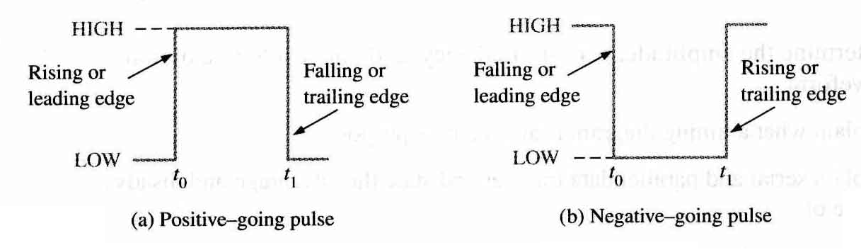
The Pulse As indicated in Figure 1-6, a pulse has two edges: a leading edge that occurs first at time $t_0$ and a trailing edge that occurs last at time $t_1$. For a positive-going pulse, the leading edge is a rising edge, and the trailing edge is a falling edge. The pulses in Figure 1-6 are ideal because the rising and falling edges are assumed to change in zero time (instantaneously). In practice, these transitions never occur instantaneously, although for most digital work you can assume ideal pulses.
Nonideal Pulse
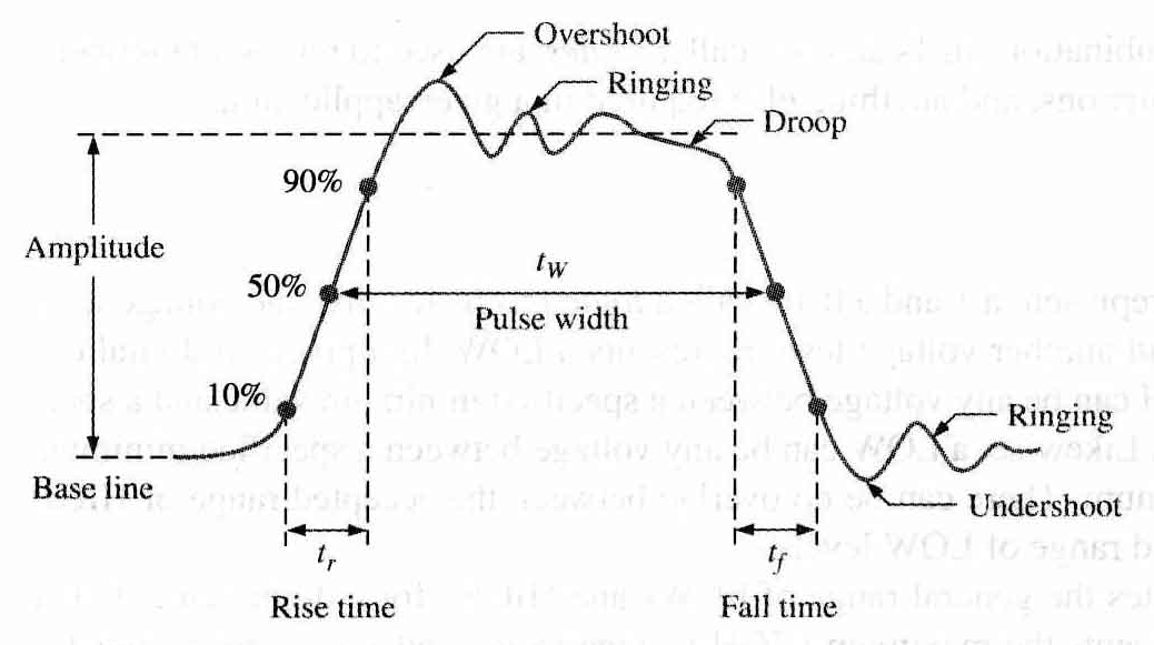
- The time required for a pulse to go from its LOW level to its HIGH level is called the rise time ($t_r$)
- The time required for the transition from the HIGH level to the LOW level is called the fall time ($t_f$)
- In practice, it is common to measure rise time from 10% of the pulse amplitude (height from baseline) to 90% of the pulse amplitude and to measure the fall time from 90% to 10% of the pulse amplitude, as indicated in Figure 1-7.
- The bottom 10% and the top 10% of the pulse are not included in the rise and fall times because of the nonlinearities in the waveform in these areas.
- The pulse width ($t_w$) is a measure of the duration of the pulse and is often defined as the time interval between the 50% points on the rising and falling edges, as indicated in Figure 1-7.
Waveform Characteristics
- A periodic pulse waveform is one that repeats itself at a fixed interval, called a period ($T$).
- The frequency ($f$) is the rate at which it repeats itself and ismeasured in hertz ($\mathrm{Hz}$).
- The duty cycle is the ratio of the pulse width ($t_{W}$) to the period ($T$) . It can be expressed as a percentage.
The Clock
In digital systems, all waveforms are synchronized with a basic timing wave-form called the clock. The clock is a periodic waveform in which each interval between pulses (the period) equals the time for one bit.
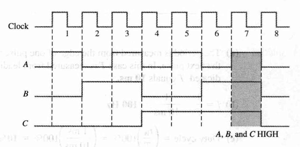
Timing Diagrams(时序图)
- A timing diagram is a graph of digital waveforms showing the actual time relationship of two or more waveforms and how each waveform changes in relation to the others.
- By looking at a timing diagram, you can determine the states (HIGH or LOW) of all the waveforms at any specified point in time and the exact time that a wave-form changes state relative to the other waveforms.
Data Transfer
Serial transfer(串行传输)
When bits are transferred in serial from one point to another, they are sent one bit at a time along a single conductor. To transfer n bits in series, it takes n time intervals.
Parallel transfer(并行传输)
When bits are transferred in parallel form, all the bits in a group are sent out on separate lines at the same time. There is one line for each bit. To transfer n bits in parallel, it takes one time interval.
Basic Logic Operations
Chapter 2 Number Systems, Operation and Codes
Number Systems
Decimal Numbers
略
Binary Numbers
略(LSB、MSB)
Binary-to-Decimal Conversion
略
Decimal-to-Binary Conversion
略
Converting Decimal Fractions to Binary
略
Binary Arithmetic
略
Signed Numbers
The Sign Bit
The left-most bit in a signed binary number is the sign bit, which tells you whether the number is positive or negative.
A 0 sign bit indicates a positive number, and a 1 sign bit indicates a negative number.
Sign-Magnitude Form
When a signed binary number is represented in sign-magnitude, the left-most bit is the sign bit and the remaining bits are the magnitude bits.
In the sign-magnitude form, a negative number has the same magnitude bits as the corresponding positive number but the sign bit is a 1 rather than a zero.
★Complements of Binary Numbers
1’s Complement (Code)
The 1’s complement(反数) of a binary number is found by changing all 1s to 0s and all 0s to 1s.
2’s Complement (Code)
The 2’s complement(补数) of a binary number is found by adding 1 to the LSB of the 1’s complement.
1’s Complement Form(反码)
Positive numbers in 1’s complement form are represented the same way as the positive sign-magnitude numbers. Negative numbers, however, are the 1’s complements of the corresponding positive numbers.(或者符号位不变,其他位取反)
2’s Complement Form(补码)
Positive numbers in 2’s complement form are represented the same way as in the signmagnitude and 1’s complement forms. Negative numbers are the 2’s complements of the corresponding positive numbers.(或者符号位不变,其他位取反+1)
Arithmetic Operations With Signed Numbers
略
Hexademical Numbers
Binary-to-Hexadecmal Conversion
略
Hexadecirmmal-to-Binary Conversion
略
Hexadecimal-to-Decimal Conversion
略
Decimal-to-Hexadecimal Conversion
略
Hexadecimal Arithmetic Operations
略
Octal Numbers
Octal-to-Decimal Conversion
略
Decimal-to-Octal Conversion
略
Octal-to-Binary Conversion
略
Binary-to-Octal Conversion
略
Binary Coded Decimal
The 8421 BCD Code
The 8421 code is a type of BCD (binary coded decimal) code. Binary coded decimal means that each decimal digit, 0 through 9, is represented by a binary code of four bits. The designation 8421 indicates the binary weights of the four bits. The ease of conversion between 8421 code numbers and the familiar decimal numbers is the main advantage of this code.
BCD Addition
BCD is a numerical code and can be used in arithmetic operations. Addition is the most important operation because the other three operations (subtraction, multiplication, and division) can be accomplished by the use of addition. Here is how to add two BCD
numbers:
- Add the two BCD numbers, using the rules for binary addition in Section 2–4.
- If a 4-bit sum is equal to or less than 9, it is a valid BCD number.
- If a 4-bit sum is greater than 9, or if a carry out of the 4-bit group is generated, it is an invalid result. Add 6 (0110) to the 4-bit sum in order to skip the six invalid states and return the code to 8421. If a carry results when 6 is added, simply add the carry to the next 4-bit group. (无效再加6,如果在加6时产生进位,只需将进位加到下一个4位组。)
Digital Codes
The Gray Code
The Gray code is unweighted and is not an arithmetic code; that is, there are no specific weights assigned to the bit positions. The important feature of the Gray code is that it exhibits only a single bit change from one code word to the next in sequence. This property is important in many applications, such as shaft position encoders, where error susceptibility increases with the number of bit changes between adjacent numbers in a sequence.
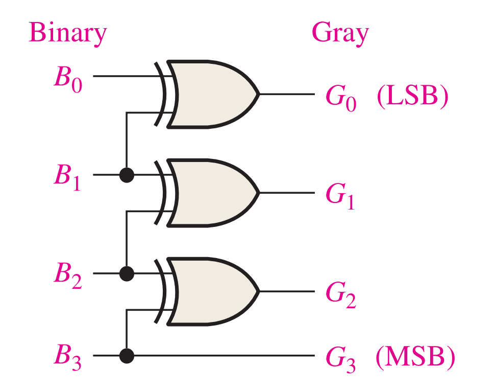
Binary-to-Gray Code Conversion
Conversion between binary code and Gray code is sometimes useful. The following rules explain how to convert from a binary number to a Gray code word:
- The most significant bit (left-most) in the Gray code is the same as the corresponding MSB in the binary number.
- Going from left to right, add each adjacent pair of binary code bits to get the next Gray code bit. Discard carries.(相邻两个相加得到格雷码对应位)
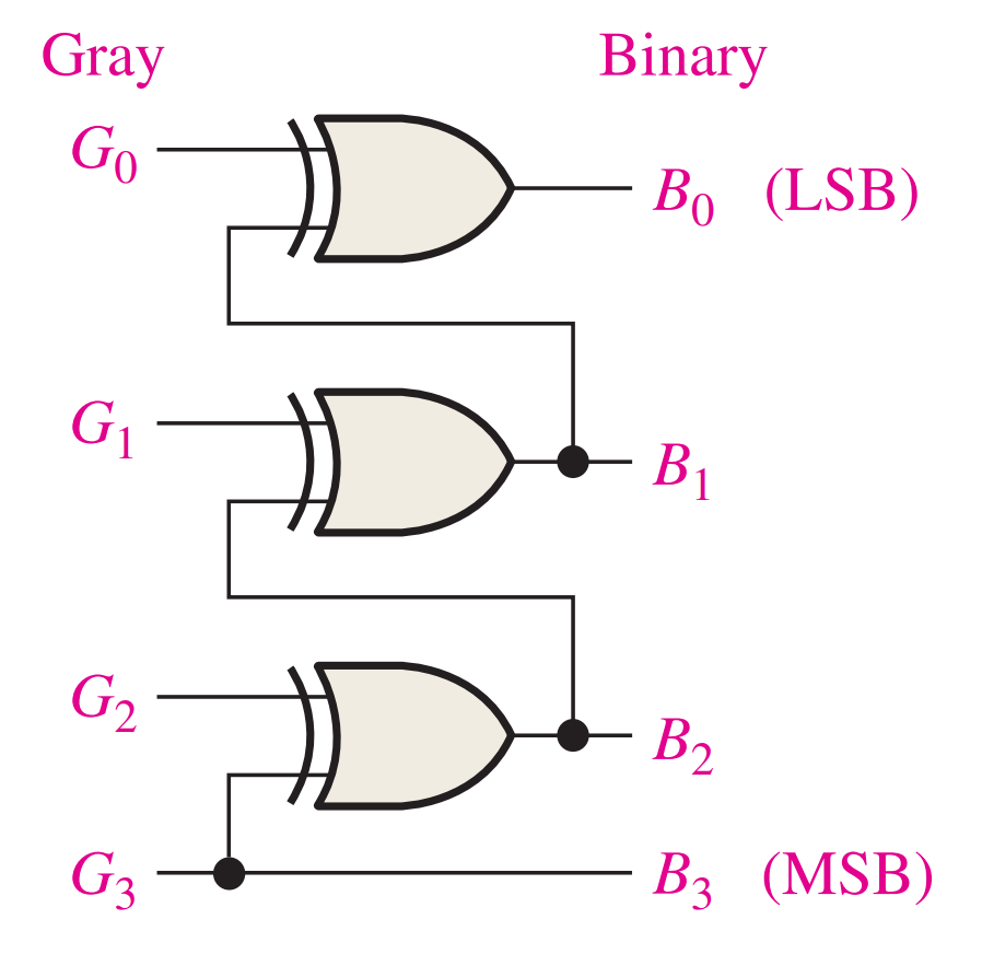
Gray-to-Binary Code Conversion
To convert from Gray code to binary, use a similar method; however, there are some differences. The following rules apply:
- The most significant bit (left-most) in the binary code is the same as the corresponding bit in the Gray code.
- Add each binary code bit generated to the Gray code bit in the next adjacent position. Discard carries.

Error Codes
Parity Method for Error Detection(错误检测的奇偶校验法)
Many systems use a parity bit as a means for bit error detection. Any group of bits contain either an even or an odd number of 1s. A parity bit is attached to a group of bits to make the total number of 1s in a group always even or always odd. An even parity bit makes the total number of 1s even, and an odd parity bit makes the total odd.(even parity bit 使总的 1 的个数(包括校验位)是偶数)
Chapter 3 Logic Gates
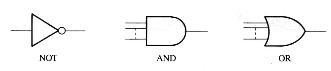
The inverter (NOT circuit)(逆变器/非门)
The inverter (NOT circuit) performs the operation called inversion or complementation. The inverter changes one logic level to the opposite level. In terms of bits, it changes a 1 to a 0 and a 0 to a 1.
Standard Symbols & Truth Table

The Negation and Polarity Indicators
The negation indicator is a “bubble” ($\circ$) that indicates inversion or complementation when it appears on the input or output of any logic element, as shown in Figure 3–1(a) for the inverter. Generally, inputs are on the left of a logic symbol and the output is on the right.
When appearing on the input, the bubble means that a 0 is the active or asserted input state, and the input is called an active-LOW input. When appearing on the output, the bubble means that a 0 is the active or asserted output state, and the output is called an active-LOW output. The absence of a bubble on the input or output means that a 1 is the active or asserted state, and in this case, the input or output is called active-HIGH.
The AND Gate
An AND gate produces a HIGH output only when all of the inputs are HIGH. When any of the inputs is LOW, the output is LOW.
Standard Symbols & Truth Table

The OR Gate
An OR gate produces a HIGH on the output when any of the inputs is HIGH. The output is
LOW only when all of the inputs are LOW.
Standard Symbols & Truth Table

The NAND Gate
The term NAND is a contraction of NOT-AND and implies an AND function with a complemented (inverted) output. The standard logic symbol for a 2-input NAND gate and its equivalency to an AND gate followed by an inverter.
Standard Symbols & Truth Table

The NOR Gate
The term NOR is a contraction of NOT-OR and implies an OR function with an inverted (complemented) output. The standard logic symbol for a 2-input NOR gate and its equivalent OR gate followed by an inverter
Standard Symbols & Truth Table

The Exclusive-OR Gate
The output of an exclusive-OR gate is HIGH only when the two inputs are at opposite logic levels.
Standard Symbols & Truth Table

The Exclusive-NOR Gate
The bubble on the output of the XNOR symbol indicates that its output is opposite that of the XOR gate. When the two input logic levels are opposite, the output of the exclusive-NOR gate is LOW.
Standard Symbols & Truth Table

Chapter 4 Boolean Algebra and Logic Simplification
Terms in Boolean Algebra
- A variable(变量) is a symbol (usually an italic uppercase letter or word) used to represent an action, a condition, or data. Any single variable can have only a 1 or a 0 value.
- The complement(补) is the inverse of a variable and is indicated by a bar over the variable (overbar). For example, the complement of the variable $A$ is $\bar{A}$. The complement of the variable A is read as “not A” or “A bar.”
- A literal(字) is a variable or the complement of a variable.
Boolean Operations and Expressions
Boolean Addition
A sum term is a sum of literals. In logic circuits, a sum term is produced by an OR operation with no AND operations involved.
Boolean Multiplication
A product term is the product of literals. In logic circuits, a product term is produced by an AND operation with no OR operations involved.
Laws of Boolean Algebra
Laws |
Equation |
For |
|---|---|---|
Commutative Laws 交换律 |
$\begin{array}{c}A + B = B + A\\AB=BA\end{array}$ |
Addition and Multiplication |
Associative Laws 结合律 |
$\begin{array}{c}A+(B+C)=(A+B)+C\\A(BC)=(AB)C\end{array}$ |
Addition and Multiplication |
Distributive Law 分配律 |
$\begin{array}{c}A(B + C) = AB + AC\\(A+B)C = AC + BC\end{array}$ |
/ |
Rules of Boolean Algebra
- $AB+\bar{A}C+BC=AB+\bar{A}C$
DeMorgan’s Theorems(德摩根定律)
- First theorem
The complement of a product of variables is equal to the sum of the complements of the variables.
The complement of two or more ANDed variables is equivalent to the OR of the complements of the individual variables. - Second theorem
The complement of a sum of variables is equal to the product of the complements of the variables.
The complement of two or more ORed variables is equivalent to the AND of the complements of the individual variables.
Standard Forms of Boolean Expressions
SOP找1,POS找0
The Sum-of-Products (SOP) Form
When two or more product terms are summed by Boolean addition, the resulting expression is a sum-of-products (SOP).
In an SOP expression, a single overbar cannot extend over more than one variable; however, more than one variable in a term can have an overbar.
Domain of a Boolean Expression
The domain of a general Boolean expression is the set of variables contained in the expression in either complemented or uncomplemented form.
The Standard SOP Form
A standard SOP expression is one in which all the variables in the domain appear in each product term in the expression.
Any nonstandard SOP expression (referred to simply as SOP) can be converted to the standard form using Boolean algebra.
Converting Product Terms to Standard SOP
Each product term in an SOP expression that does not contain all the variables in the domain can be expanded to standard form to include all variables in the domain and their complements.
Step 1: Multiply each nonstandard product term by a term made up of the sum of a missing variable and its complement. This results in two product terms. As you know, you can multiply anything by 1 without changing its value.(缺失变量的项乘以 $1$,$1$ 变成 $A+\bar{A}$,再用分配律展开)
Step 2: Repeat Step 1 until all resulting product terms contain all variables in the domain in either complemented or uncomplemented form. In converting a product term to standard form, the number of product terms is doubled for each missing variable.
Binary Representation of a Standard Product Term
The product term has a binary value 使对应的 Term 值为 1
The Product-of-Sums (POS) Form
When two or more sum terms are multiplied, the resulting expression is a product-of-sums (POS).
In a POS expression, a single overbar cannot extend over more than one variable; however, more than one variable in a term can have an overbar.
The Standard POS Form
A standard POS expression is one in which all the variables in the domain appear in each sum term in the expression.
Any nonstandard POS expression (referred to simply as POS) can be converted to the standard form using Boolean algebra.
Converting a Sum Term to Standard POS
Each sum term in a POS expression that does not contain all the variables in the domain can be expanded to standard form to include all variables in the domain and their complements.
Step 1: Add to each nonstandard product term a term made up of the product of the missing variable and its complement. This results in two sum terms. As you know, you can add 0 to anything without changing its value.(缺失变量的项加上 $0$,$0$ 变成 $A\cdot\bar{A}$,再用 $A + BC = (A + B)(A + C)$ 展开)
Step 2: Apply rule 12 : $A + BC = (A + B)(A + C)$
Step 3: Repeat Step 1 until all resulting sum terms contain all variables in the domain in either complemented or uncomplemented form.
Binary Representation of a Standard Sum Term
The sum term has a binary value 使对应的 Term 值为 0
Converting Standard SOP to Standard POS
The binary values of the product terms in a given standard SOP expression are not present in the equivalent standard POS expression. Also, the binary values that are not represented in the SOP expression are present in the equivalent POS expression.
Step 1: Evaluate each product term in the SOP expression. That is, determine the binary numbers that represent the product terms.(积的binary value是让积为1的数)
Step 2: Determine all of the binary numbers not included in the evaluation in Step 1.
Step 3: Write the equivalent sum term for each binary number from Step 2 and express in POS form.
Converting SOP Expressions to Truth Table Format
- First in constructing a truth table is to list all possible combinations of binary values of the variables in the expression.
- Next, convert the SOP expression to standard form if it is not already.
- Finally, place a 1 in the output column (X) for each binary value that makes the standard SOP expression a 1 and place a 0 for all the remaining binary values.
Converting POS Expressions to Truth Table Format
- First list all the possible combinations of binary values of the variables just as was done for the SOP expression.
- Next, convert the POS expression to standard form if it is not already.
- Finally, place a 0 in the output column (X) for each binary value that makes the expression a 0 and place a 1 for all the remaining binary values.
Determining Standard Expressions from a Truth Table
To determine the standard SOP expression represented by a truth table, list the binary values of the input variables for which the output is 1. Convert each binary value to the corresponding product term by replacing each 1 with the corresponding variable and each 0 with the corresponding variable complement.
To determine the standard POS expression represented by a truth table, list the binary values for which the output is 0. Convert each binary value to the corresponding sum term by replacing each 1 with the corresponding variable complement and each 0 with the corresponding variable.
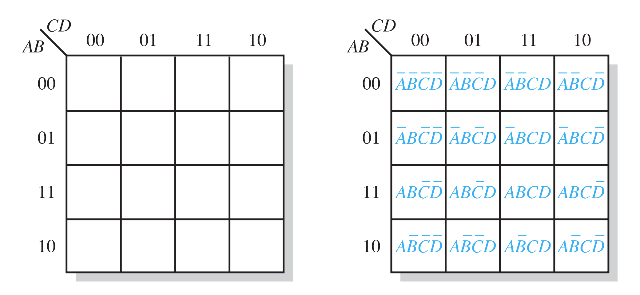
The Karnaugh Map(卡诺图)
A Karnaugh map provides a systematic method for simplifying Boolean expressions and, if properly used, will produce the simplest SOP or POS expression possible, known as the minimum expression.
A Karnaugh map is similar to a truth table because it presents all of the possible values of input variables and the resulting output for each value. Instead of being organized into columns and rows like a truth table, the Karnaugh map is an array of cells in which each cell represents a binary value of the input variables. The cells are arranged in a way so that simplification of a given expression is simply a matter of properly grouping the cells. Karnaugh maps can be used for expressions with two, three, four, and five variables, but we
will discuss only 3-variable and 4-variable situations to illustrate the principles.
The 3-Variable Karnaugh Map

The 4-Variable Karnaugh Map
Cell Adjacency
The cells in a Karnaugh map are arranged so that there is only a single-variable change between adjacent cells. Adjacency is defined by a single-variable change.
- A cell is not adjacent to the cells that diagonally touch any of its corners.(对角线不相邻)
- Also, the cells in the top row are adjacent to the corresponding cells in the bottom row.(首尾行相连)
- And the cells in the outer left column are adjacent to the corresponding cells in the outer right column.(首尾列相邻)
- This is called “wrap-around” adjacency(“环绕式”邻接) because you can think of the map as wrapping around from top to bottom to form a cylinder or from left to right to form a cylinder.
Karnaugh Map SOP Minimization
A minimized SOP expression contains the fewest possible terms with the fewest possible variables per term.
Steps One : Mapping a Standard SOP Expression
Determine the binary value of each product term in the standard SOP expression. As each product term is evaluated, place a 1 on the Karnaugh map in the cell having the same value as the product term.
For an SOP expression in standard form, a 1 is placed on the Karnaugh map for each product term in the expression. Each 1 is placed in a cell corresponding to the value of a product term.
Step Two : Grouping the 1s
- A group must contain either 1, 2, 4, 8, or 16 cells, which are all powers of two. In the case of a 3-variable map, 2^3 = 8 cells is the maximum group.(总数是 2 的幂)
- Each cell in a group must be adjacent to one or more cells in that same group, but all cells in the group do not have to be adjacent to each other.(长方形)
- Always include the largest possible number of 1s in a group in accordance with rule 1.(长方形最大化)
- Each 1 on the map must be included in at least one group. The 1s already in a group can be included in another group as long as the overlapping groups include noncommon 1s.(所有 1 都要进组,可以进多组)
Step Three : Determining the Minimum SOP Expression from the Map
- Each group of cells containing 1s creates one product term composed of all variables that occur in only one form (either uncomplemented or complemented) within the group. Variables that occur both uncomplemented and complemented within the group are eliminated. These are called contradictory variables
- Determine the minimum product term for each group.
- For a 3-variable map:
- A 1-cell group yields a 3-variable product term
- A 2-cell group yields a 2-variable product term
- A 4-cell group yields a 1-variable term
- An 8-cell group yields a value of 1 for the expression
- For a 4-variable map:
- A 1-cell group yields a 4-variable product term
- A 2-cell group yields a 3-variable product term
- A 4-cell group yields a 2-variable product term
- An 8-cell group yields a 1-variable term
- A 16-cell group yields a value of 1 for the expression
- For a 3-variable map:
“Don’t Care” Conditions
Sometimes a situation arises in which some input variable combinations are not allowed. The “don’t care” terms can be used to advantage on the Karnaugh map. For each “don’t care” term, an X is placed in the cell. When grouping the 1s, the Xs can be treated as 1s to make a larger grouping or as 0s if they cannot be used to advantage. The larger a group, the simpler the resulting term will be.
Karnaugh Map POS Minimization
Steps One : Mapping a Standard POS Expression
Determine the binary value of each sum term in the standard POS expression. This is the binary value that makes the term equal to 0. As each sum term is evaluated, place a 0 on the Karnaugh map in the corresponding cell.
For a POS expression in standard form, a 0 is placed on the Karnaugh map for each sum term in the expression. Each 0 is placed in a cell corresponding to the value of a sum term.
Step Two : Grouping the 1s
The process for minimizing a POS expression is basically the same as for an SOP expression except that you group 0s to produce minimum sum terms instead of grouping 1s to produce minimum product terms.
Step Three : Determining the Minimum POS Expression from the Map
Converting Between POS and SOP Using the Karnaugh Map
略
Chapter 5 Combinational Logic Analysis
略
Chapter 6 Functions of Combinational Logic
The Half-Adder
The half-adder accepts two binary digits on its inputs and produces two binary digits on its outputs——a sum bit($\Sigma$) and a carry bit($C_{\mathrm{out}}$).
The Full-Adder
The full-adder accepts two input bits and an input carry($C_{\mathrm{in}}$) and generates a sum output and an output carry.
Parallel Binary Adders
Two or more full-adders are connected to form parallel binary adders.
Four-Bit Parallel Adders
A group of four bits is called a nibble. A basic 4-bit parallel adder is implemented with four full-adder stages as shown in Figure 6–9. Again, the LSBs (A1 and B1) in each number being added go into the right-most full-adder; the higher-order bits are applied as shown to the successively higher-order adders, with the MSBs (A4 and B4) in each number being applied to the left-most full-adder. The carry output of each adder is connected to the carry input of the next higher-order adder as indicated. These are called internal carries.

Adder Expansion
The 4-bit parallel adder can be expanded to handle the addition of two 8-bit numbers by
using two 4-bit adders.
The Ripple Carry Adder(串行进位加法器)
A ripple carry adder is one in which the carry output of each full-adder is connected to the carry input of the next higher-order stage (a stage is one full-adder). The sum and the output carry of any stage cannot be produced until the input carry occurs; this causes a time delay in the addition process.
The Look-Ahead Carry Adder(超前进位加法器)
The look-ahead carry adder anticipates the output carry of each stage, and based on the inputs, produces the output carry by either carry generation or carry propagation.
原理略
Comparators
The basic function of a comparator is to compare the magnitudes of two binary quantities to determine the relationship of those quantities. In its simplest form, a comparator circuit determines whether two numbers are equal.
Equality
In order to produce a single output indicating an equality or inequality of two numbers, an AND gate can be combined with XNOR gates, as shown in Figure 6–19. The output of each exclusive-NOR gate is applied to the AND gate input. When the two input bits for each exclusive-NOR are equal, the corresponding bits of the numbers are equal, producing a 1 on both inputs to the AND gate and thus a 1 on the output. When the two numbers are not equal, one or both sets of corresponding bits are unequal, and a 0 appears on at least one input to the AND gate to produce a 0 on its output. Thus, the output of the AND gate indicates equality (1) or inequality (0) of the two numbers.
Inequality
略
芯片实现
Use 74HC85 comparators to compare the magnitudes of two 8-bit numbers.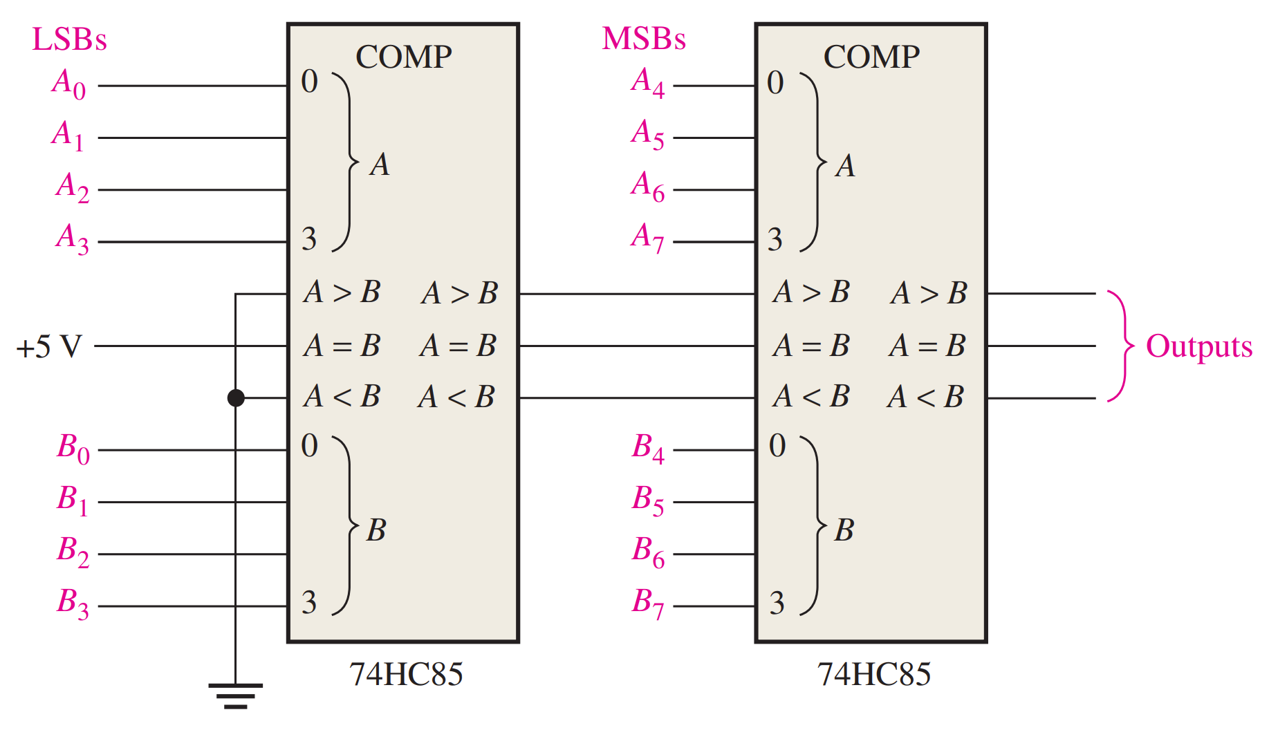
Decoders
A decoder is a digital circuit that detects the presence of a specified combination of bits (code) on its inputs and indicates the presence of that code by a specified output level. In its general form, a decoder has $n$ input lines to handle $n$ bits and from one to $2^n$ output lines to indicate the presence of one or more $n$-bit combinations.
The 4-Bit Decoder
In order to decode all possible combinations of four bits, sixteen decoding gates are required ($2^4 = 16$). This type of decoder is commonly called either a 4-line-to-16-line decoder because there are four inputs and sixteen outputs or a 1-of-16 decoder because for any given code on the inputs, one of the sixteen outputs is activated.
芯片实现
The 74HC154 is a good example of a fixed-function IC decoder. There is an enable function (EN) provided on this device, which is implemented with a NOR gate used as a negative-AND. A LOW level on each chip select input, CS1 and CS2, is required in order to make the enable gate output (EN) HIGH. The enable gate output is connected to an input of each NAND gate in the decoder, so it must be HIGH for the NAND gates to be enabled. If the enable gate is not activated by a LOW on both inputs, then all sixteen decoder outputs (OUT) will be HIGH regardless of the states of the four input variables.(CS1 和 CS2 全 0 才能激活芯片,未激活时输入全为 1)
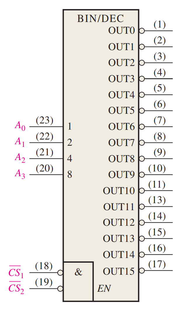
Since the 74HC154 can handle only four bits, two decoders must be used to form a
5-bit expansion.

The BCD-to-Decimal Decoder
The BCD-to-decimal decoder converts each BCD code (8421 code) into one of ten possible decimal digit indications. It is frequently referred as a 4-line-to-10-line decoder or a 1-of-10 decoder
芯片实现
The 74HC42 is a fixed-function IC decoder with four BCD inputs and ten active-LOW decimal outputs.

The BCD-to-7-Segment Decoder
The BCD-to-7-segment decoder accepts the BCD code on its inputs and provides outputs to drive 7-segment display devices to produce a decimal readout.
芯片实现
The 74HC47 is an example of an IC device that decodes a BCD input and drives a 7-segment display. In addition to its decoding and segment drive capability, the 74HC47 has several additional features as indicated by the $\bar{LT}$, $\bar{RBI}$, $\bar{BI}/\bar{RBO}$ functions in the logic symbol of Figure 6–34. As indicated by the bubbles on the logic symbol, all of the outputs (a through g) are active-LOW as are the $\bar{LT}$ (lamp test), $\bar{RBI}$ (ripple blanking input), and $\bar{BI}/\bar{RBO}$ (blanking input/ripple blanking output) functions. The outputs can drive a common-anode 7-segment display directly. Recall that 7-segment displays were discussed in Chapter 4. In addition to decoding a BCD input and producing the appropriate 7-segment outputs, the 74HC47 has lamp test and zero suppression capability.($\bar{LT}$ 灯管检查,全部都输出 1;$\bar{RBI}$ 为 active 时且 BCD 输入为 0 时,全部输出 0,同时 $\bar{RBO}$ 输出 active)
Zero Suppression for a 4-Digit Display
leading zero suppression
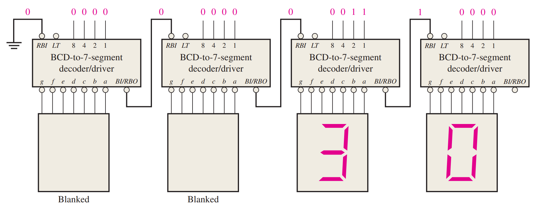
trailing zero suppression

Encoders
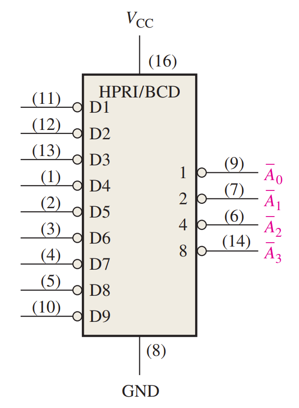
The Octal-to-Binary Priority Encoder
The 74F148 is a 8-Line-to-3-line priority encoder that has eight active-LOW inputs and three active-LOW binary outputs. The device can be used for converting octal inputs to a 3-bit binary code.

- $\bar{EI}$:Enable Input. When inactive, all outputs are deactivated.(激活芯片)
- $\bar{EO}$:Enable output. $\bar{EO}$ is active if $\bar{EI}$ is active and none of the inputs is active.(指示芯片激活且没输入)
- $\bar{GS}$:Gate Strobe. $\bar{GS}$ is active if $\bar{EI}$ is active and any of the inputs is active.(指示芯片激活且有输入)
Expansion: 16-4 Priority Encoder

The Decimal-to-BCD Priority Encoder
This type of encoder performs the same basic encoding function as previously discussed. A priority encoder also offers additional flexibility in that it can be used in applications that require priority detection. The priority function means that the encoder will produce a BCD output corresponding to the highest-order decimal digit input that is active and will ignore any other lower-order active inputs. For instance, if the 6 and the 3 inputs are both active, the BCD output is 0110 (which represents decimal 6).
芯片实现
The 74HC147 is a priority encoder with active-LOW inputs (0) for decimal digits 1 through 9 and active-LOW BCD outputs. A BCD zero output is represented when none of the inputs is active.
Code Converters
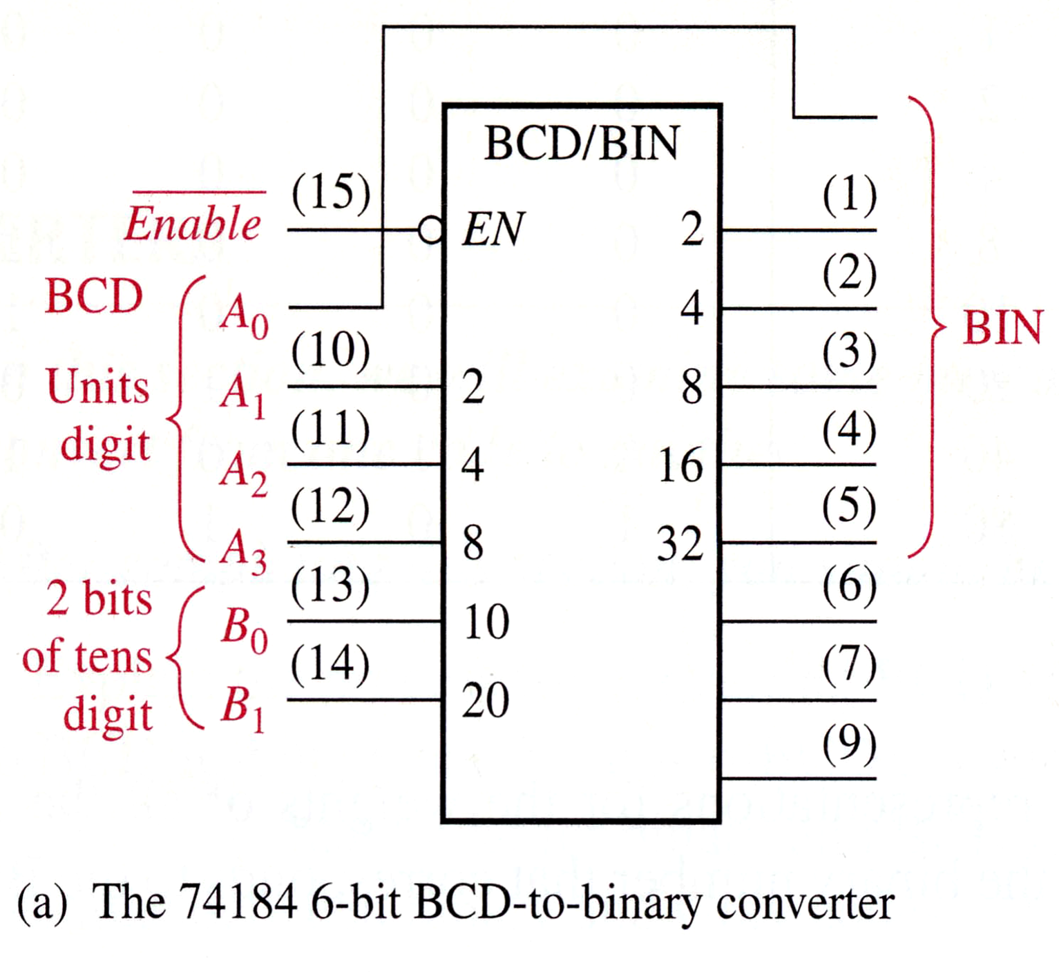
BCD-to-Binary Conversion
Steps:
- Determine the value or weight of each bit in the BCD number, and represent it by a binary number
- Add all the weights that the corresponding bits are 1s
- The result of this addition is the binary equivalent of the BCD number
芯片实现
Binary-to-Gray Conversion
Gray-to-Binary Conversion
Multiplexers (Data Selectors)
A multiplexer (MUX) is a device that allows digital information from several sources to be routed onto a single line for transmission over that line to a common destination. The basic multiplexer has several data-input lines and a single output line. It also has data-select inputs, which permit digital data on any one of the inputs to be switched to the output line. Multiplexers are also known as data selectors.
Logic expression
芯片实现
An MSI 8-input Multiplexer (74HC151)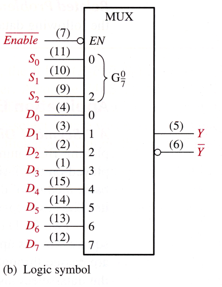
The 74HC153 is a dual four-input data selector/multiplexer.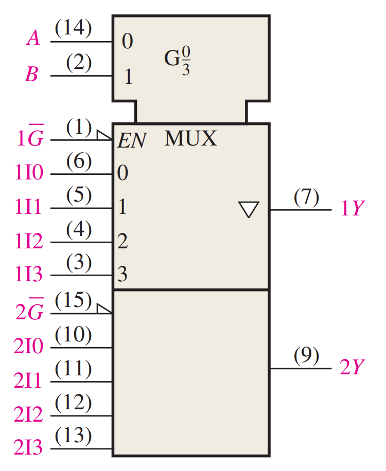
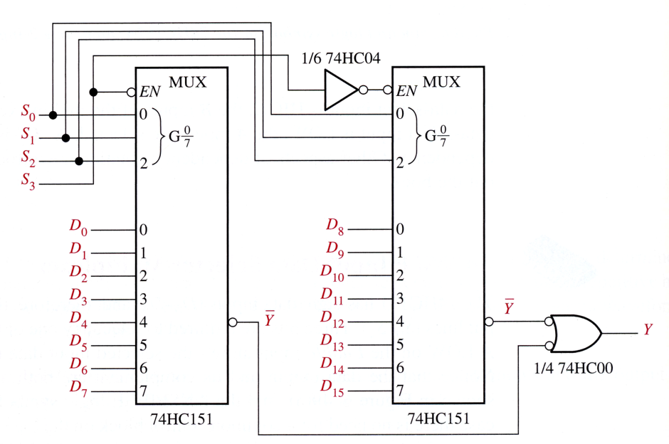
Expansion: 16-inputs multiplexer
Demultiplexers (Data Distributors)
A demultiplexer (DEMUX) basically reverses the multiplexing function. It takes digital information from one line and distributes it to a given number of output lines. For this reason, the demultiplexer is also known as a data distributor. As you will learn, decoders can also be used as demultiplexers.
芯片实现
An MSI 4-16 Demultiplexer (74HC154)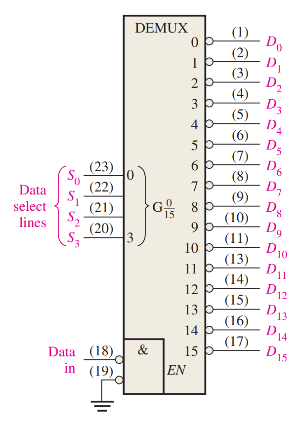
Parity Generators/Checkers
An MSI 9-bit Parity Generator/Checker-74LS280(生成校验码)
This particular device can be used to check for odd or even parity on a 9-bit code (eight data bits and one parity bit), or it can be used to generate a parity bit for a binary code with up to nine bits. The inputs are A through I; when there is an even number of 1s on the inputs, the $\Sigma$ Even output is HIGH and the $\Sigma$ Odd output is LOW.

- When this device is used as an even parity checker, the number of input bits should always be even; and when a parity error occurs, the $\Sigma$ Even output goes LOW and the $\Sigma$ Odd output goes HIGH. When it is used as an odd parity checker, the number of input bits should always be odd; and when a parity error occurs, the $\Sigma$ Odd output goes LOW and the $\Sigma$ Even output goes HIGH.
- If this device is used as an even parity generator, the parity bit is taken at the $\Sigma$ Odd output because this output is a 0 if there is an even number of input bits and it is a 1 if there is an odd number. When used as an odd parity generator, the parity bit is taken at the $\Sigma$ Even output because it is a 0 when the number of inputs bits is odd.
Chapter 7 Latches, Flip-Flops, and Timers
Bistable devices(双稳态)
Bistable devices have two stable states, called SET and RESET; they can retain either of these states indefinitely, making them useful as storage devices.
Monostable devices(单稳态)
The monostable multivibrator, commonly known as the one-shot, has only one stable state.
Astable devices(无稳态)
The astable multivibrator has no stable state and is used primarily as an oscillator, which is a self-sustained waveform generator.
Latches
The latch(锁存器) is a type of temporary storage device that has two stable states (bistable) and is normally placed in a category separate from that of flip-flops. Latches are similar to flip-flops because they are bistable devices that can reside in either of two states using a feedback arrangement, in which the outputs are connected back to the opposite inputs. The main difference between latches and flip-flops is in the method used for changing their state.
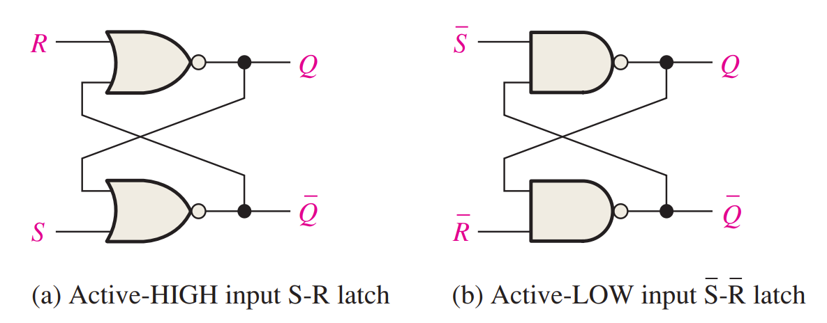
The S-R (SET-RESET) Latch
A latch is a type of bistable logic device or multivibrator. An active-HIGH input S-R (SET-RESET) latch is formed with two cross-coupled NOR gates; an active-LOW input S-R latch is formed with two cross-coupled NAND gates. Notice that the output of each gate is connected to an input of the opposite gate. This produces the regenerative feedback(负反馈) that is characteristic of all latches and flip-flops.
Truth table for an active-LOW input $\bar{S}-\bar{R}$ latch
The Gated S-R Latch
A gated latch requires an enable input, EN (G is also used to designate an enable input). The logic diagram and logic symbol for a gated S-R latch are shown in Figure 7–8. The S and R inputs control the state to which the latch will go when a HIGH level is applied to the EN input.
The latch will not change until EN is HIGH; but as long as it remains HIGH, the output is controlled by the state of the S and R inputs. The gated latch is a level-sensitive device. In this circuit, the invalid state occurs when both S and R are simultaneously HIGH and EN is also HIGH.
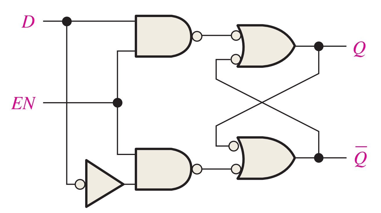
The Gated D Latch
Another type of gated latch is called the D latch. It differs from the S-R latch because it has only one input in addition to EN. This input is called the D (data) input. The following figure contains a logic diagram and logic symbol of a D latch. When the D input is HIGH and the EN input is HIGH, the latch will set. When the D input is LOW and EN is HIGH, the latch will reset. Stated another way, the output Q follows the input D when EN is HIGH.
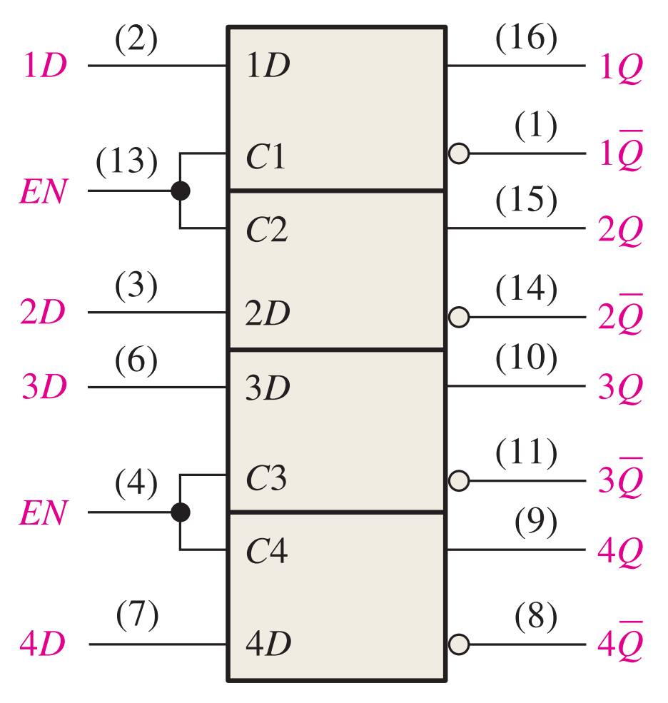
芯片实现
An example of a gated D latch is the 74HC75 represented by the logic symbol in Figure 7–12(a). The device has four latches. Notice that each active-HIGH EN input is shared by two latches and is designated as a control input (C). The truth table for each latch is shown in Figure 7–12(b). The X in the truth table represents a “don’t care” condition. In this case, when the EN input is LOW, it does not matter what the D input is because the outputs are unaffected and remain in their prior states.
Flip-Flops
Flip-flops are synchronous bistable devices(同步双稳态设备), also known as bistable multivibrators(双稳态多纤颤器). In this case, the term synchronous means that the output changes state only at a specified point (leading or trailing edge) on the triggering input called the clock (CLK), which is designated as a control input, C; that is, changes in the output occur in synchronization with the clock. Flip-flops are edge-triggered or edge-sensitive whereas gated latches are level-sensitive.
Edge-triggered flip-flop
An edge-triggered flip-flop changes state either at the positive edge (rising edge) or at the negative edge (falling edge) of the clock pulse and is sensitive to its inputs only at this transition of the clock. Two types of edge-triggered flip-flops are covered in this section: D and J-K. The logic symbols for these flip-flops are shown in Figure 7–13. Notice that each type can be either positive edge-triggered (no bubble at C input) or negative edge-triggered (bubble at C input). The key to identifying an edge-triggered flip-flop by its logic symbol is the small triangle inside the block at the clock (C) input. This triangle is called the dynamic input indicator.
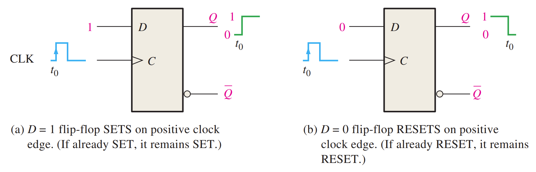
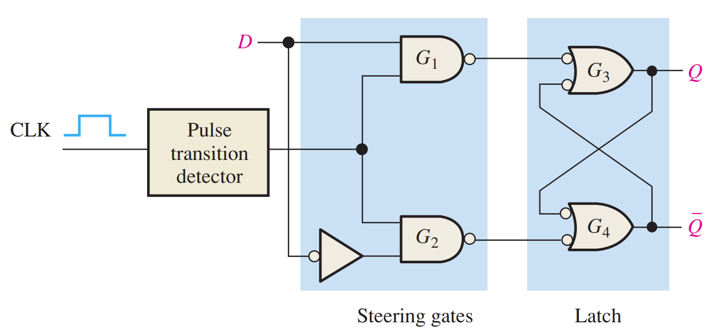
The D Flip-Flop
The D input of the D flip-flop is a synchronous input because data on the input are transferred to the flip-flop’s output only on the triggering edge of the clock pulse.
- When D is HIGH, the Q output goes HIGH on the triggering edge of the clock pulse, and the flip-flop is SET.
- When D is LOW, the Q output goes LOW on the triggering edge of the clock pulse, and the flip-flop is RESET.
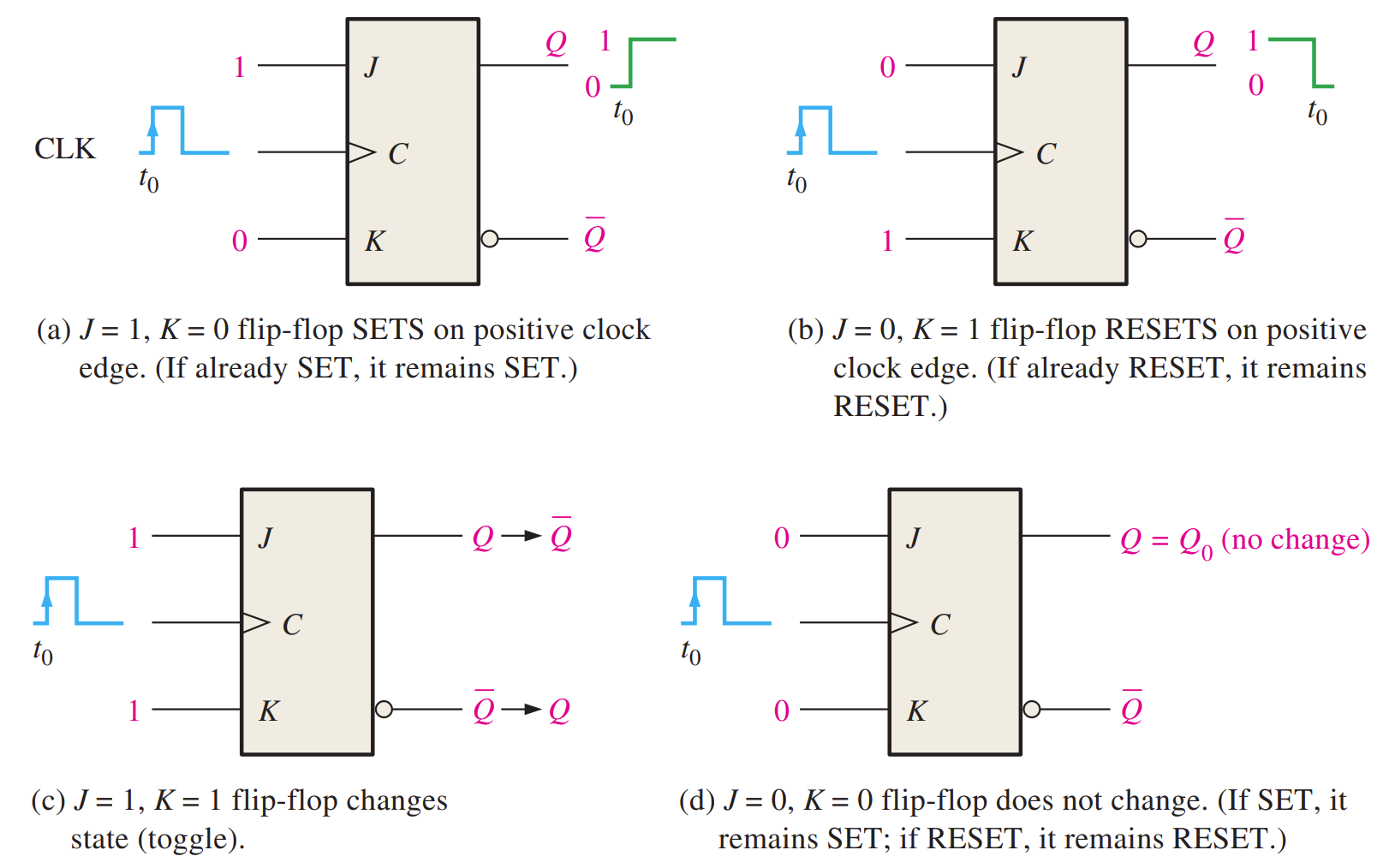
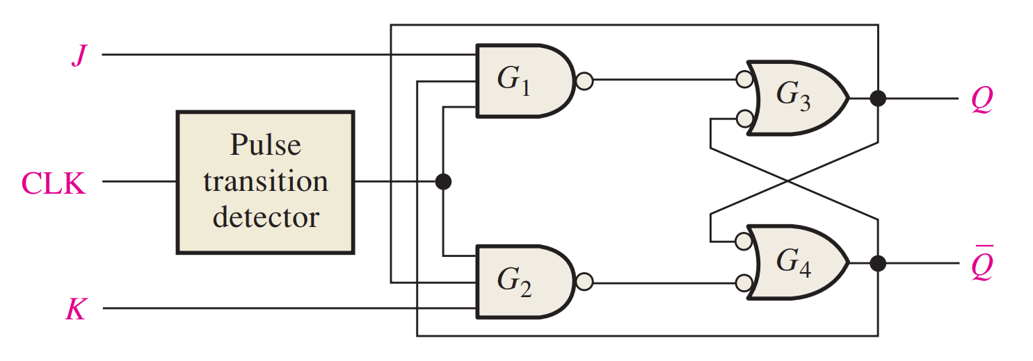
The J-K Flip-Flop
The J and K inputs of the J-K flip-flop are synchronous inputs because data on these inputs are transferred to the flip-flop’s output only on the triggering edge of the clock pulse.
- When J is HIGH and K is LOW, the Q output goes HIGH on the triggering edge of the clock pulse, and the flip-flop is SET.
- When J is LOW and K is HIGH, the Q output goes LOW on the triggering edge of the clock pulse, and the flip-flop is RESET.
- When both J and K are LOW, the output does not change from its prior state.
- When J and K are both HIGH, the flip-flop changes state. This called the toggle mode.
Edge-Triggered Operation(内部实现)
D Flip-Flop
J-K Flip-Flop
Asynchronous Preset and Clear Inputs(不由时钟控制)

芯片实现
(Todo)
Flip-Flop Applications
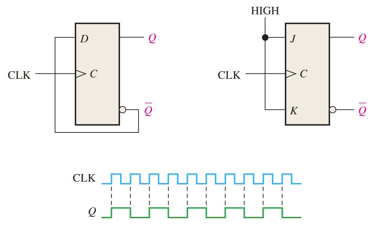
Parallel Data Storage

Frequency Division
Counting

One-Shots
The one-shot, also known as a monostable multivibrator(单稳态多谐振荡器), is a device with only one stable state. A one-shot is normally in its stable state and will change to its unstable state only when triggered. Once it is triggered, the one-shot remains in its unstable state for a predetermined length of time and then automatically returns to its stable state. The time that the device stays in its unstable state determines the pulse width of its output.
(Todo)
The Astable Multivibrator
An astable multivibrator is a device that has no stable states; it changes back and forth (oscillates(震荡)) between two unstable states without any external triggering. The resulting output is typically a square wave that is used as a clock signal in many types of sequential logic circuits. Astable multivibrators are also known as pulse oscillators.
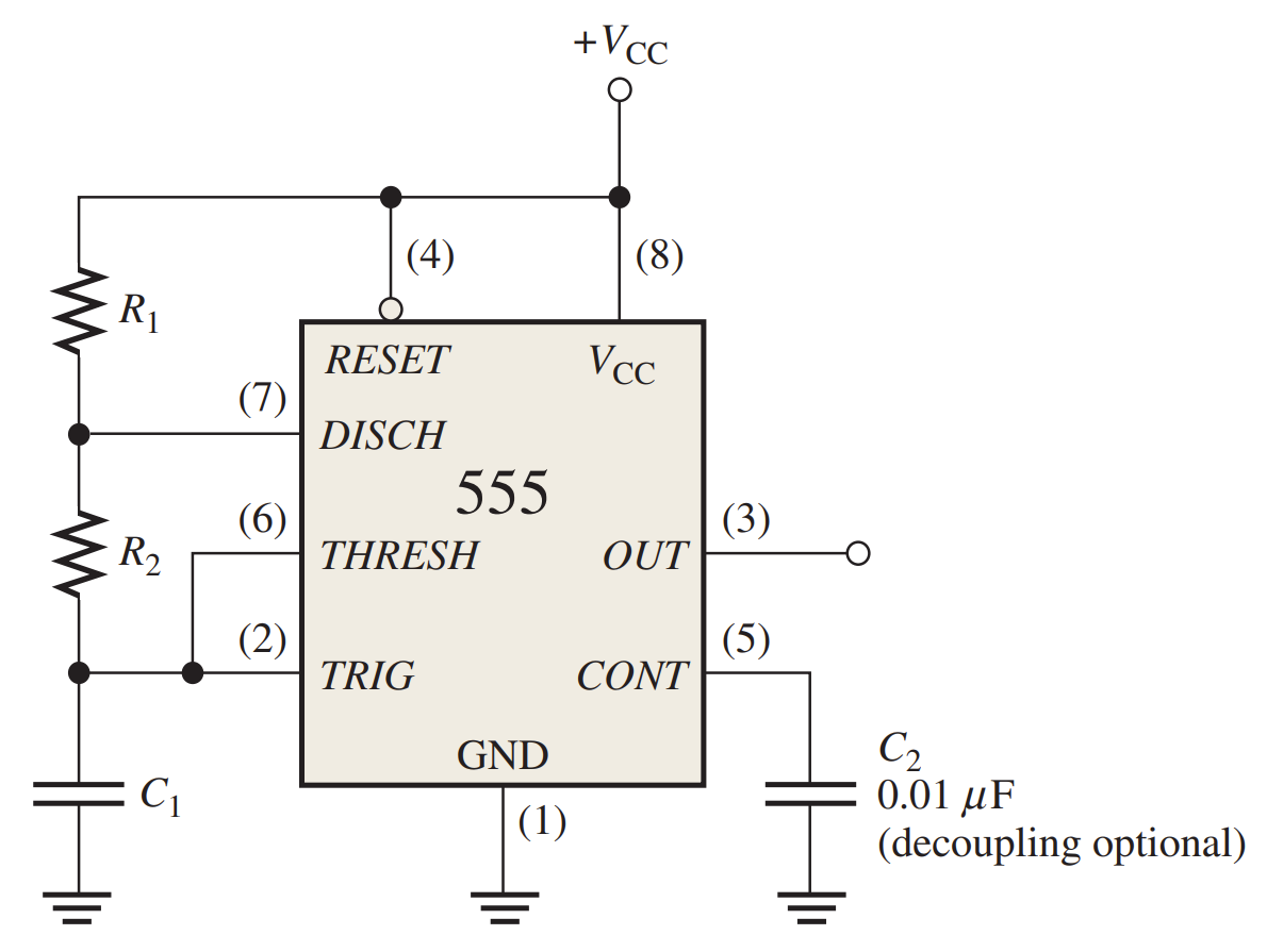
The 555 Timer
Intro
The 555 timer is a versatile and widely used IC device because it can be configured in two different modes as either a monostable multivibrator (one-shot) or as an astable multivibrator (pulse oscillator)(非稳态多谐振荡器).
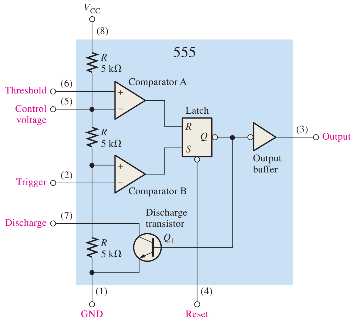
Monostable (One-Shot) Operation

- The pulse width of the output is determined by the time constant of $R_1$ and $C_1$ according to the following formula: $t_{W}=1.1 R_1 C_1$
- Before a trigger pulse is applied, the output is LOW and the discharge transistor $Q_1$ is on, keeping $C_1$ discharged.
- When a negative-going trigger pulse is applied at $t_0$, the output goes HIGH and the discharge transistor turns off, allowing capacitor $C_1$ to begin charging through $R_1$.
- When $C_1$ charges to $1/3 V_{CC}$, the output goes back LOW at $t_1$ and $Q_1$ turns on immediately, discharging $C_1$.
As an Astable Multivibrator
Chapter 8 Counters
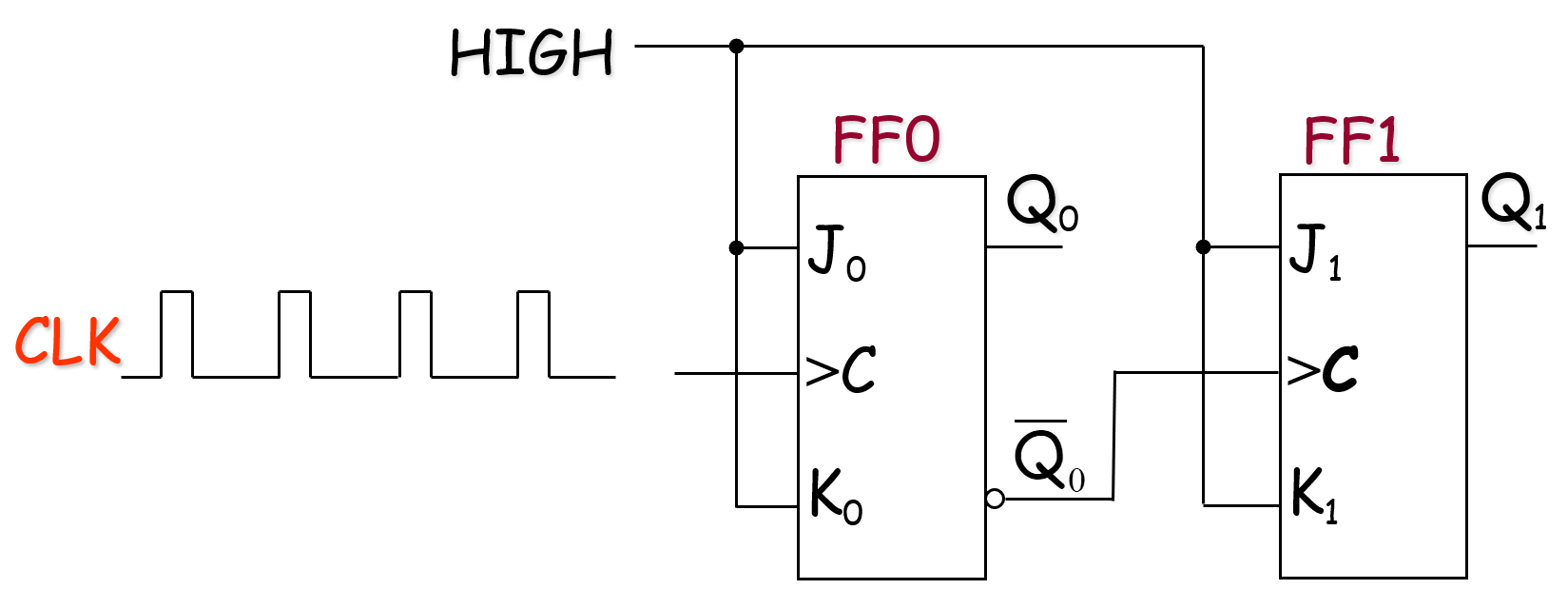
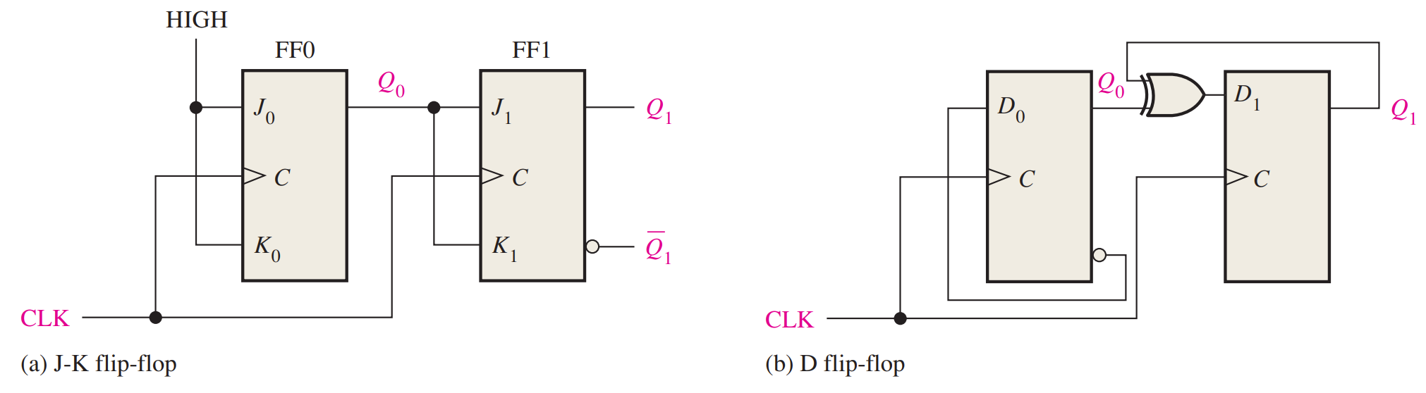
Asynchronous Counters
The term asynchronous refers to events that do not have a fixed time relationship with each other and, generally, do not occur at the same time. An asynchronous counter is one in which the flip-flops (FF) within the counter do not change states at exactly the same time because they do not have a common clock pulse.
A 2-Bit Asynchronous Binary Counter

A 3-Bit Asynchronous Binary Counter

Propagation Delay(传播时延)
Asynchronous counters are commonly referred to as ripple counters for the following reason: The effect of the input clock pulse is first “felt” by FF0. This effect cannot get to FF1 immediately because of the propagation delay through FF0. Then there is the propagation delay through FF1 before FF2 can be triggered. Thus, the effect of an input clock pulse “ripples” through the counter, taking some time, due to propagation delays, to reach the last flip-flop.
This cumulative delay of an asynchronous counter is a major disadvantage in many applications because it limits the rate at which the counter can be clocked and creates decoding problems. The maximum cumulative delay in a counter must be less than the period of the clock waveform.
Asynchronous Decade Counters
The modulus(模) of a counter is the number of unique states through which the counter will sequence. The maximum possible number of states (maximum modulus) of a counter is $2^n$, where $n$ is the number of flip-flops in the counter. Counters can be designed to have a number of states in their sequence that is less than the maximum of $2^n$. This type of sequence is called a truncated sequence.
Partial Decoding

芯片实现
(Todo)
Synchronous Counters
The term synchronous refers to events that have a fixed time relationship with each other. A synchronous counter is one in which all the flip-flops in the counter are clocked at the same time by a common clock pulse. J-K flip-flops are used to illustrate most synchronous counters. D flip-flops can also be used but generally require more logic because of having no direct toggle or no-change states.
A 2-Bit Synchronous Binary Counter
A 3-Bit Synchronous Binary Counter
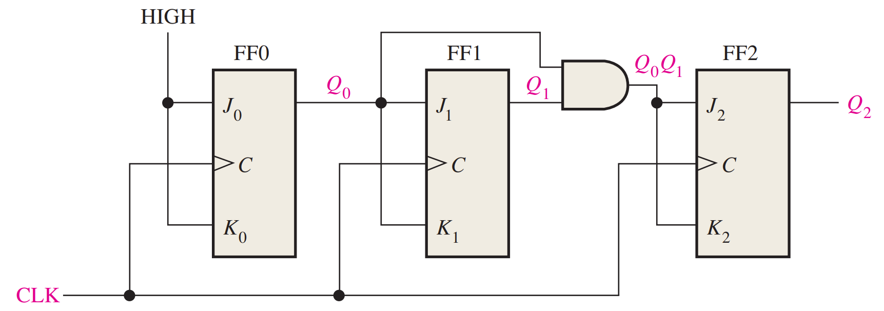
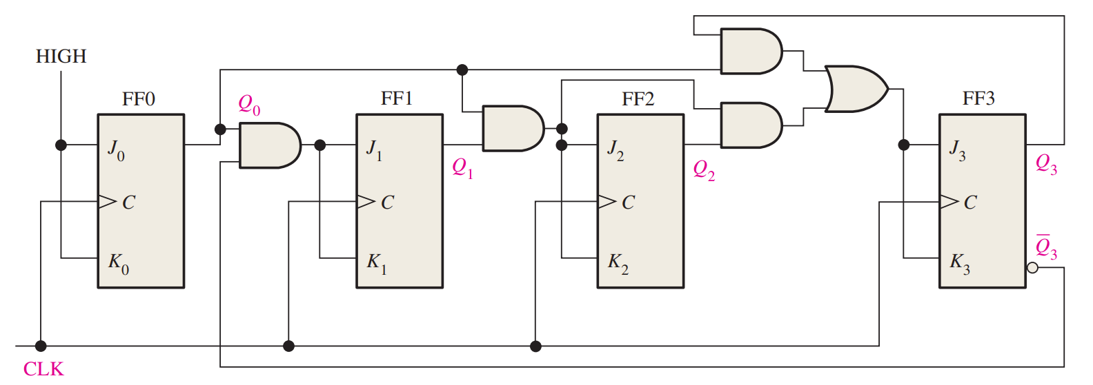
A 4-Bit Synchronous Binary Counter

芯片实现
The 74HC163 is an example of an integrated circuit 4-bit synchronous binary counter.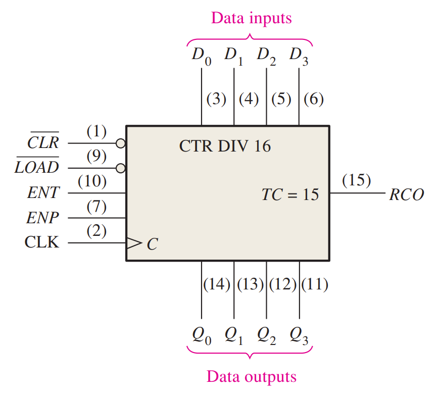
- When a LOW is applied to the $\overline{LOAD}$ input, the counter will assume the state of the data inputs on the next clock pulse.
- there is an active-LOW clear input ($\overline{CLR}$), which synchronously resets all four flip-flops in the counter.
- There are two enable inputs, $ENP$ and $ENT$. These inputs must both be HIGH for the counter to sequence through its binary states. When at least one input is LOW, the counter is disabled.
- The ripple clock output ($RCO$) goes HIGH when the counter reaches the last state in its sequence of fifteen, called the terminal count($TC = 15$).
A synchronous BCD decade counter
Up/Down Synchronous Counters
An up/down counter is one that is capable of progressing in either direction through a certain sequence. An up/down counter, sometimes called a bidirectional counter, can have any specified sequence of states.
A basic 3-bit up/down synchronous counter

芯片实现
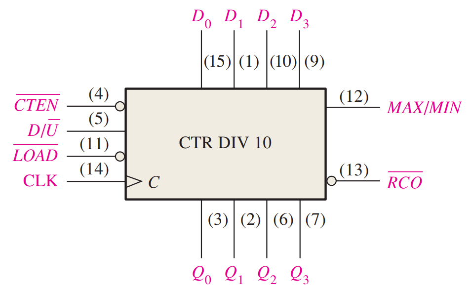
- The 74HC190, an example of an integrated circuit up/down synchronous decade counter.
- The direction of the count is determined by the level of the up/down input ($D/\overline{U}$). When this input is HIGH, the counter counts down; when it is LOW, the counter counts up.
- Also, this device can be preset to any desired BCD digit as determined by the states of the data inputs when the $\overline{LOAD}$ input is LOW.
- The $MAX/MIN$ output produces a HIGH pulse when the terminal count nine (1001) is reached in the UP mode or when the terminal count zero (0000) is reached in the DOWN mode.
Design of Synchronous Counters
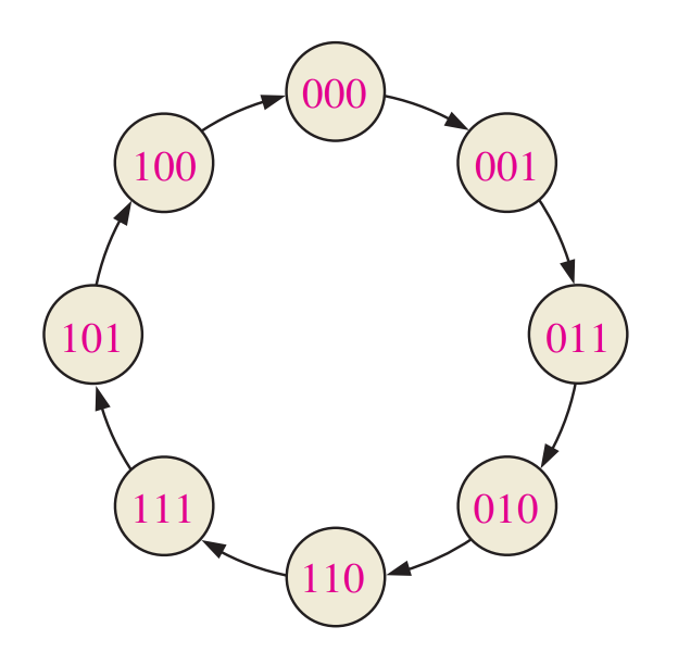
Step 1: State Diagram
A state diagram shows the progression of states through which the counter advances when it is clocked.
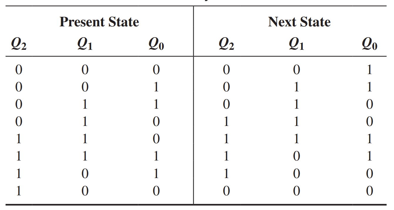
Step 2: Next-State Table
Once the sequential circuit is defined by a state diagram, the second step is to derive a next-state table, which lists each state of the counter (present state) along with the corresponding next state. The next state is the state that the counter goes to from its present
state upon application of a clock pulse.
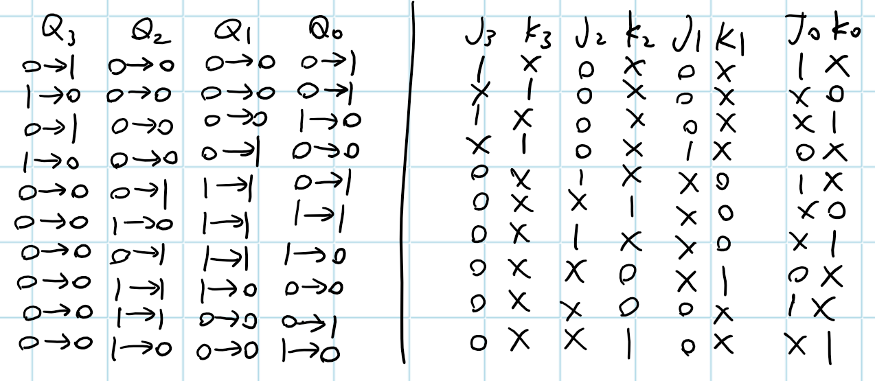
Step 3: Flip-Flop Transition Table
All possible output transitions are listed by showing the Q output of the flip-flop going from present states to next states. QN is the present state of the flip-flop (before a clock pulse) and QN + 1 is the next state (after a clock pulse). For each output transition, the J and K inputs that will cause the transition to occur are listed. An X indicates a “don’t care”

Step 4: Karnaugh Maps
Karnaugh maps can be used to determine the logic required for the J and K inputs of each flip-flop in the counter. There is a Karnaugh map for the J input and a Karnaugh map for the K input of each flip-flop. In this design procedure, each cell in a Karnaugh map represents one of the present states in the counter sequence listed in Next-State Table.
Step 5: Logic Expressions for Flip-Flop Inputs
From the Karnaugh maps you obtain the expressions for the J and K inputs of each flip-flop
Step 6: Counter Implementation
The final step is to implement the combinational logic from the expressions for the J and K inputs and connect the flip-flops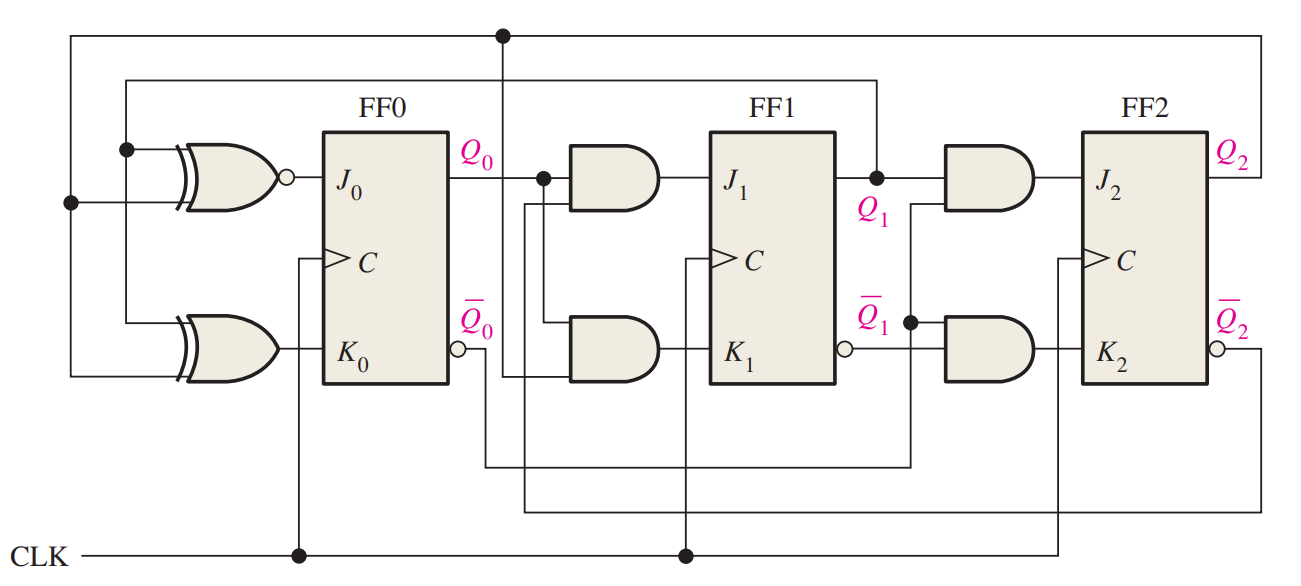
Design of Synchronous Counters(方法二)
Step 1: State Diagram
Step 2: Next-State Table
Step 3: Karnaugh Maps for Next State of Counter
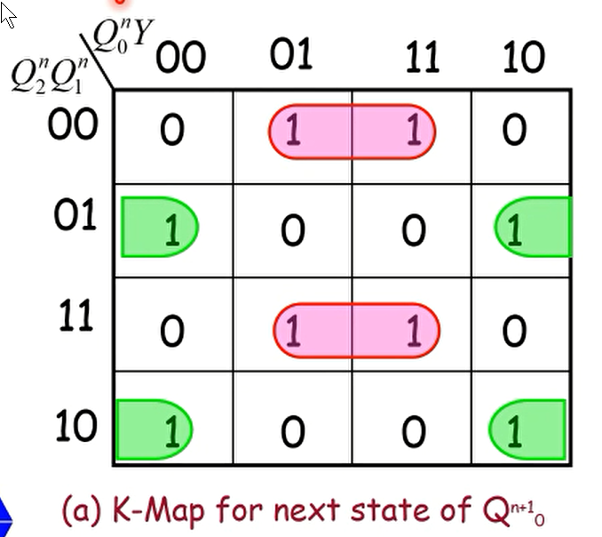
用上一个状态的输出Q(有UP/DOWN的话再加Y)导出下一个状态的每个Qn
Step 4: Logic Expressions for Flip-Flop Inputs
先把 $Q_{i}^{n+1}$ 化成 SOP 形式,再与上式比较,得出 $J_i$ 与 $K_i$
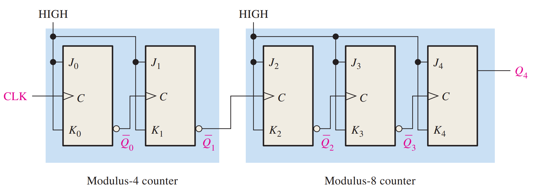
Cascaded Counters
Asynchronous Cascading

Synchronous Cascading

Decoding Glitches
The propagation delays(传播延时) due to the ripple effect in asynchronous counters create transitional states in which the counter outputs are changing at slightly different times. These transitional states produce undesired voltage spikes of short duration (glitches) on the outputs of a decoder connected to the counter. The glitch problem can also occur to some degree with synchronous counters because the propagation delays from the clock to the Q outputs of each flip-flop in a counter can vary slightly.
One way to eliminate the glitches is to enable the decoded outputs at a time after the glitches have had time to disappear. This method is known as strobing and can be accomplished in the case of an active-HIGH clock by using the LOW level of the clock to enable
the decoder.

Counter Applications
电子表从01到12的计数
本博客所有文章除特别声明外,均采用 CC BY-NC-ND 4.0 协议 ,转载请注明出处!